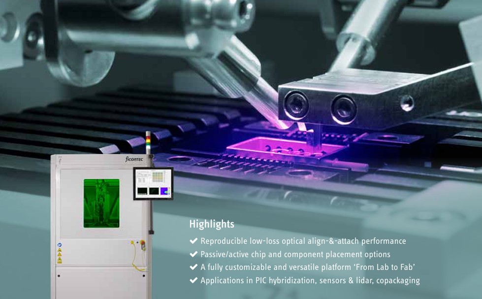


Fully automated, industry-qualified assembly for optoelectronics and singulated photonic devices and PICs. Featuring high-precision ‘align-&-attach’ bonding capability for all optical elements, fibers and arrays, as well as for die, chip or PIC integration and hybridization.
A highly capable development and/or batch processing platform, uniquely combining high-precision optical alignment capability with a multiplicity of bonding technologies. Designed for all optical, fiber and die/chip/PIC connection and hybridization tasks.
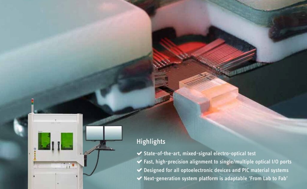
Fully automated, mixed-signal electro-optical test systems for optoelectronics and singulated photonic devices. Featuring DC, RF and optical measurements in a production-optimized modular layout, and targeted at R&D, volume manufacturing, and anything in between.
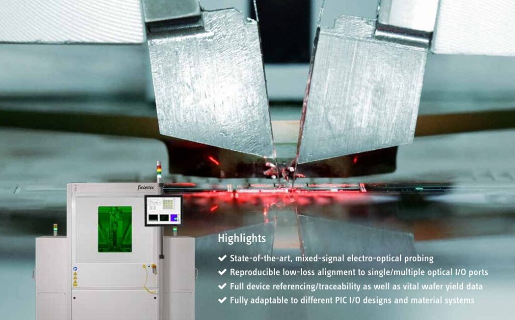
Innovative mixed-signal electro-optical test systems for non-singulated photonic integrated circuits (PICs) and other optoelectronic devices. Featuring fully automated DC, RF and optical measurements both on-wafer and for single photonic devices on appropriate carrier formats.
Fully automated precision stacking/unstacking for semiconductor laser diode bars. Typically used in preparation for a coating process, and/or for post-process unstacking and optical inspection of facet and side walls (optional). Configurable as a stand-alone or as an in-line assembly cell.
Phone:+91-22-3504 8294